⏱️ 20-25 min read
Hope you’re all having a lovely holiday season ❄️. I wish you will do amazing things in coming revolution of the sun. Cold weather is perfect for getting cosy with a long read — or, worst case, reading my article and dozing off immediately 😄.
The topic might be a bit specific (or boring to some!), but I’m genuinely grateful for the encouragement and appreciation you showed for my first article.
Thank you for the support — it really means a lot.
TL;DR
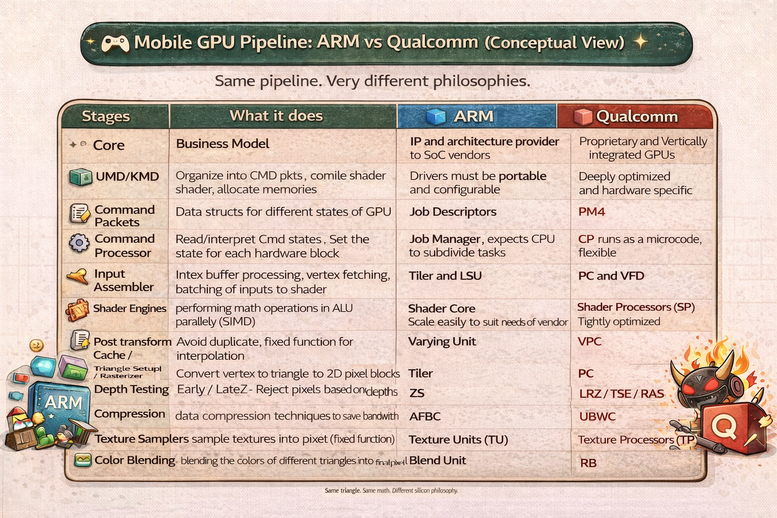
Quick recap of Part 1 — in 5 points
- What a GPU actually consumes: rendering starts with a small but powerful set of inputs — vertex buffers for structure, index buffers for efficiency, and textures for visual richness.
- How 3D becomes 2D: scene data flows through the graphics pipeline, where vertices are transformed, primitives are rasterized, and fragments eventually become pixels.
- Pipeline anatomy matters: modern graphics APIs combine fixed-function hardware for speed with programmable shaders for flexibility — each stage exists for a reason.
- Mobile GPUs live under brutal constraints: limited power and memory bandwidth force them to move away from desktop-style Immediate Mode Rendering.
- Tile-Based Rendering isn’t an optimisation: it is the architectural foundation that makes mobile GPUs possible in your hand without colling fan (ya I know phones are releasing with cooling fan these days, Honor WIN).
- Binning and on-chip tile processing change everything: by drastically reducing memory traffic, mobile GPUs can deliver sustained performance within a 2–5 W power envelope.
(…okay fine, it was 6 points. GPUs love over-subdivision anyway : ) )
Hope I’ve clearly made the case for why tiling exists.
With that foundation in place, we’re finally ready to explore how different mobile GPUs move a triangle through their pipelines — and how ARM Mali and Qualcomm Adreno take such different architectural paths to solve the same problem.
Part 2 is where the triangle really starts its journey.

Disclaimer
Before we go any further, a quick but important note.
This article does not reveal any closed-door secrets, proprietary designs, or confidential implementation details. Everything discussed here is based on public documentation, developer talks, academic material, and architectural principles commonly understood in the graphics community.

Idea of the article is to frame the comparison correctly as learning of basics.
ARM is primarily an IP and architecture provider — it designs GPU architectures that are licensed by many SoC vendors, who then integrate and tune them within their own systems.
Qualcomm, on the other hand, builds vertically integrated GPUs — designing the architecture, hardware, drivers, and software stack together to deliver fast, power-efficient mobile graphics.
Both approaches have produced industry-leading mobile GPUs in their own right.
So while we follow the journey of a triangle through a mobile GPU, the goal is not to crown a winner.
Instead, we’ll explore how different design philosophies and business models shape architectural decisions —
and how those choices manifest in areas like tiling, scheduling, visibility, and pipeline organisation.
Think of it as learning how ideology influences silicon — one triangle at a time.
Role of Application and GPU Driver
Apps—whether games, game engines, UI frameworks, home screens, messaging applications—use the GPU in one way or another. This could be for rendering animations, transitions, or different scenes on screen.
At a high level, application developers are responsible for defining the scene, preparing resources (such as vertex buffers and textures), and issuing draw calls. How these resources are allocated and how draw calls are set up has a direct impact on application performance.
That’s why GPU vendors release Developer Guides that document best practices for resource usage, draw call submission, and performance optimization. (If you haven’t read them yet, do check them out—they’re surprisingly informative.)
However, even with all this in place, the application still does not talk to the hardware directly.
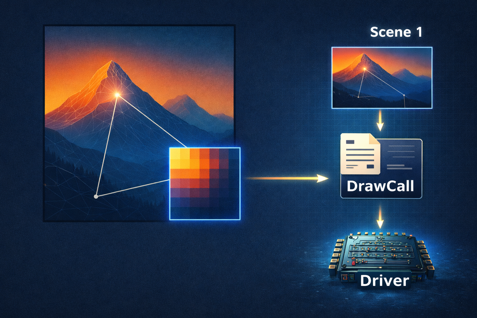
So who actually talks to the GPU?
That’s where drivers come into play.
Applications don’t communicate with GPU hardware directly. Instead, their requests flow through the graphics driver stack. For simplicity, I’ll treat the API runtime and the User-Mode Driver (UMD) as a single logical layer here.
The flow looks like this:
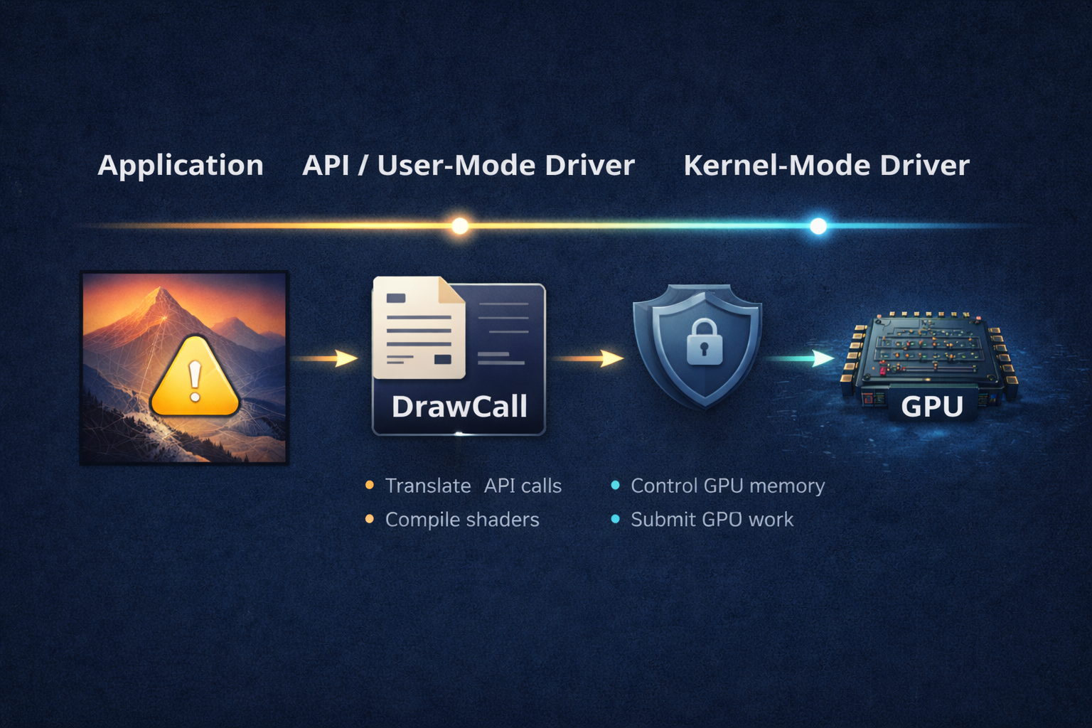
User-Mode Driver (UMD): translating intent into work
The User-Mode Driver sits closest to the application and is responsible for translating high-level API calls into something the GPU can eventually execute. Its responsibilities include:
- State Tracking
UMD maintains the current GPU state—what shaders are bound, which textures and buffers are active, blend modes, raster state, and so on. - Validation
It checks whether the application’s requests are valid and legal for the hardware (for example, ensuring resource limits aren’t exceeded or incompatible states aren’t combined). - Batching & Minor Optimizations
It may group commands or perform lightweight optimizations before handing work off downstream. - Shader Compilation
Although the API provides pre-validated shader bytecode, UMD must translate this into hardware-specific machine code. This step involves deep, low-level work such as register allocation, instruction scheduling, and target-specific optimizations. - Shader Substitution (quite infamous part)
In some cases, drivers detect known applications or games and replace their shaders with hand-tuned versions written by driver engineers to improve performance. - State “JIT-ing”
Not all API states map cleanly to hardware. When a feature isn’t directly supported, the UMD may recompile shaders on the fly, injecting extra logic to emulate that state. - Command Buffer Generation
Finally, the UMD converts API calls into streams of hardware-specific binary commands (often called command buffers or DMA buffers).
I know , you might be missing Compiler here .
Kernel-Mode Driver (KMD): owning the hardware
Once command buffers are ready, they are passed to the Kernel-Mode Driver, which has privileged access to the system and the GPU. The KMD is responsible for:
- Actual memory allocation and mapping
- Resource residency and protection
- Submitting command buffers to the GPU safely
Scheduling: sharing the GPU
GPU is a shared system resource—used simultaneously by the OS, the browser, background services, and applications. A graphics scheduler (part of the operating system) arbitrates access.
- It decides which application gets GPU time and when
- When execution switches between applications, a context switch occurs
- Context switches require saving and restoring GPU state, which is not free and directly impacts performance
Why this matters
This entire stack—UMD, KMD, and scheduling—exists to balance performance, correctness, and fairness. It also explains why the same application can behave very differently across vendors, APIs, and platforms.
⚖️ ARM vs Qualcomm — Driver Philosophy
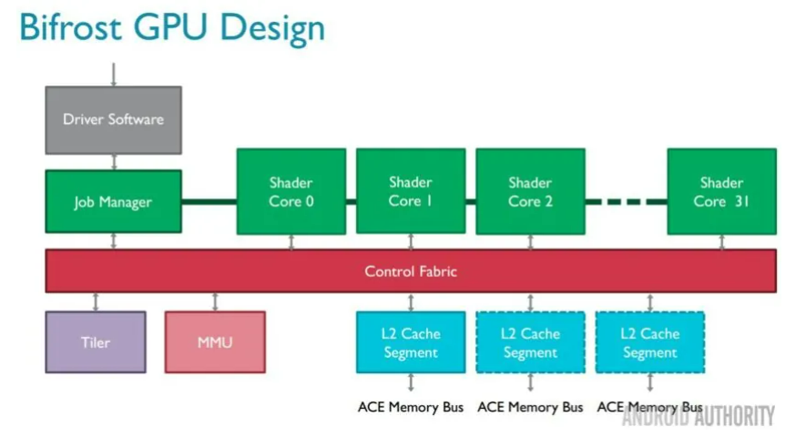
ARM does not ship end-user products. It licenses GPU IP (Mali) to many SoC vendors—Samsung, MediaTek, Rockchip, etc.
Driver implications:
- Drivers must be portable and configurable
- One codebase must work across:
- many SoCs
- different memory systems
- different firmware stacks
- ARM provides:
- reference drivers
- tuning guides
- integration hooks
👉 ARM drivers are designed to be general-purpose and adaptable, not deeply tied to one product.
Qualcomm driver development happens with vertical integration in mind (Adreno GPU, SoC, firmware, driver stack).
Driver implications:
- Drivers are hardware-specific
- Tighter control over:
- memory management
- scheduling
- power
- Lots of optimization put in to minimize the work done in GPUs
👉 Qualcomm drivers are deeply optimized for a narrow set of GPUs.
GPU Hardware Architecture
Going forward I will refer Qualcomm GPU based primarily on this diagram of Adreno 530 taken from chipsandcheese (links in resource).
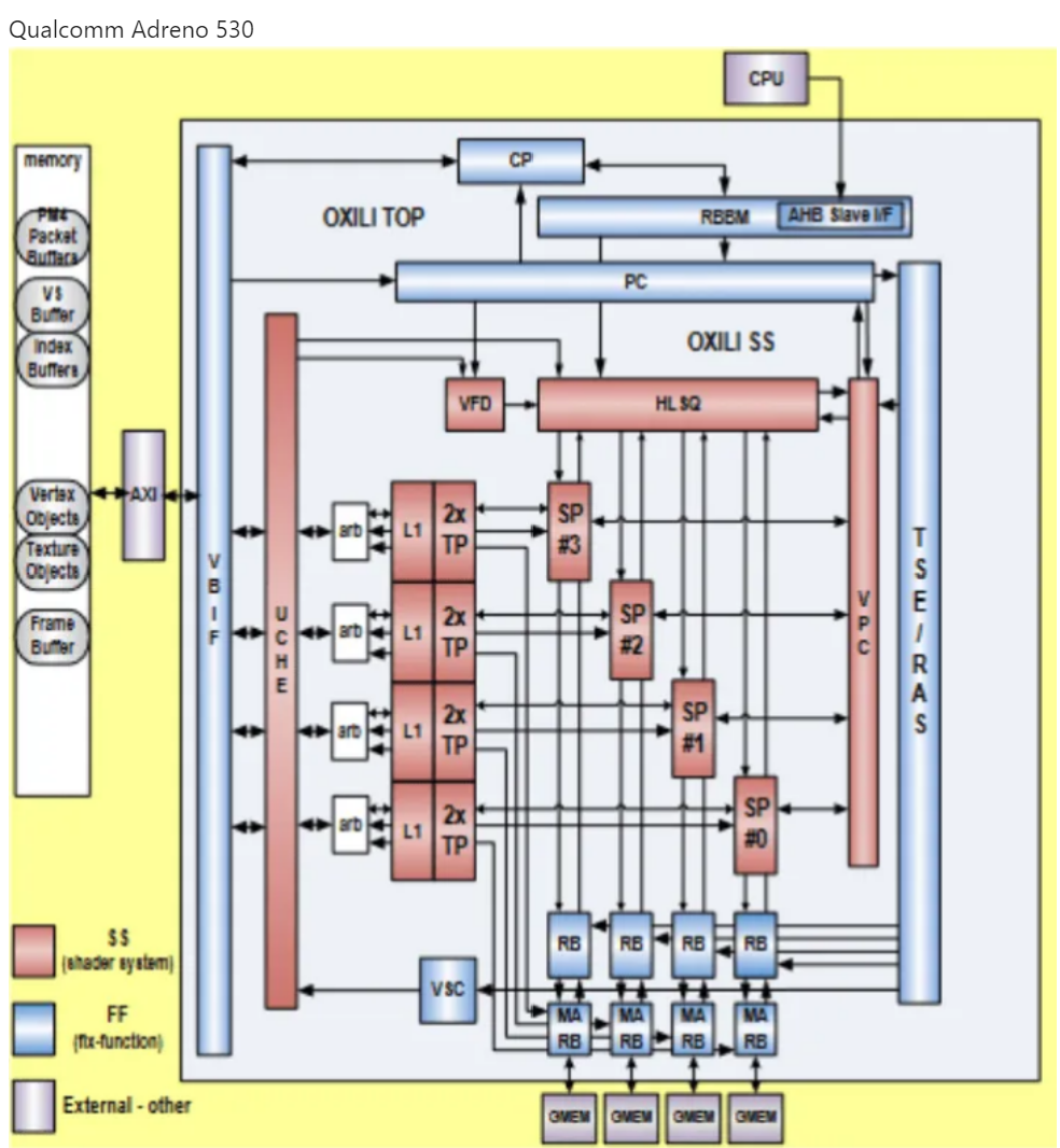
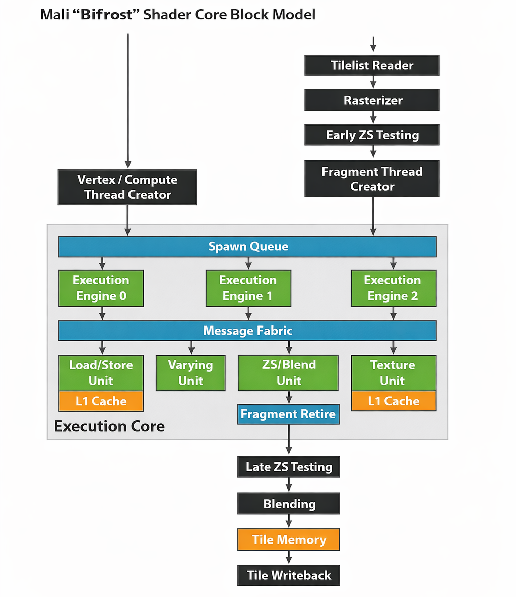
Similarly for ARM, I will be refering to their Bifrost GPU design.
Command Processor — Front End of the GPU
Our dear driver organizes all application requests—draw calls, dispatches, and synchronization—into packets. These packets are written in a proprietary, packetized command format understood by the GPU.
- Qualcomm calls these packets PM4, historically derived from ATI/AMD’s PM4 format.
- ARM uses Job Descriptors.
Each packet typically contains:
- State updates
Enabling or configuring GPU features (pipeline state, shaders, raster state, etc.) - Draw / Dispatch commands
Explicit triggers telling the GPU to execute work - Resource management & synchronization
Barriers, fences, semaphores, and ordering constraints
CPU → GPU: how commands are delivered
To send these packets to GPU, CPU writes them into memory structures that the GPU can consume. The most common mechanism is a ring buffer (circular buffer):
- CPU acts as producer, writing commands
- GPU acts as consumer, reading and executing them
Other signalling mechanisms exist, but for sustained GPU workloads, this producer–consumer model works extremely well. Polling or doorbell-style notifications are often sufficient given the GPU’s deep pipelines and long-running tasks.
Enter the Command Processor
Once the GPU begins consuming the command stream, the Command Processor (CP)—the front end of the GPU—takes over. Many people call it the brain of the GPU. I prefer calling it the stomach 🙂—because its job is to chew, digest, and route work to the rest of the GPU.
Its primary responsibility is to manage the incoming command stream so that high-throughput execution units (the shaders) never starve.
What the Command Processor actually does
The Command Processor is typically split into two major stages:
1. Fetching
- Reads command packets from memory locations written by the CPU
- Maintains ordering and flow control
2. Decoding
- Interprets binary command packets
- If the command is a Draw / Dispatch, it:
- Programs internal GPU state
- Triggers geometry, tiling, or compute engines
- If the command is a Wait / Sync, it:
- Stalls execution until a condition is satisfied
⚖️ ARM vs Qualcomm — Command Processor philosophy
ARM Mali: Job-centric front end
Traditional Mali GPUs used a Job Manager–based design.
- CPU does more upfront work
- Tasks are broken into explicit jobs
- Each job descriptor contains state for specific GPU blocks
- GPU processes jobs largely as submitted
This approach:
- Keeps hardware simpler
- Pushes more responsibility to the driver and CPU
- Makes driver efficiency and job construction critical
Qualcomm Adreno: firmware-driven command processing
Adreno GPUs have long used a more flexible, firmware-driven Command Processor.
- CP runs microcode
- It parses command streams and dynamically distributes work
- Commands can be routed to different internal GPU “slices”
- GPU behavior can evolve via firmware/driver updates without hardware changes
This enables:
- Greater scheduling flexibility
- Faster iteration on GPU logic
- Better handling of real-world, imperfect workloads
| Aspect | ARM Mali | Qualcomm Adreno |
|---|---|---|
| Front-end model | Job-based | Command stream |
| CPU responsibility | Higher | Lower |
| GPU logic | More fixed | Firmware-programmable |
| Flexibility | Driver-driven | Hardware + firmware |
| Evolution over time | Slower | Faster |
Important note
ARM’s newer architectures have evolved beyond the classic Job Manager model and now use Command Stream Front Ends, moving closer to a modern command-processor design.
Input Assembler — Hardware Front End
Input Assembler (IA) is the stage that takes raw buffers of numbers from memory and turns them into something the GPU can reason about: primitives, most commonly triangles.
Its job is not shading—it’s structuring data so the shader cores can work efficiently.
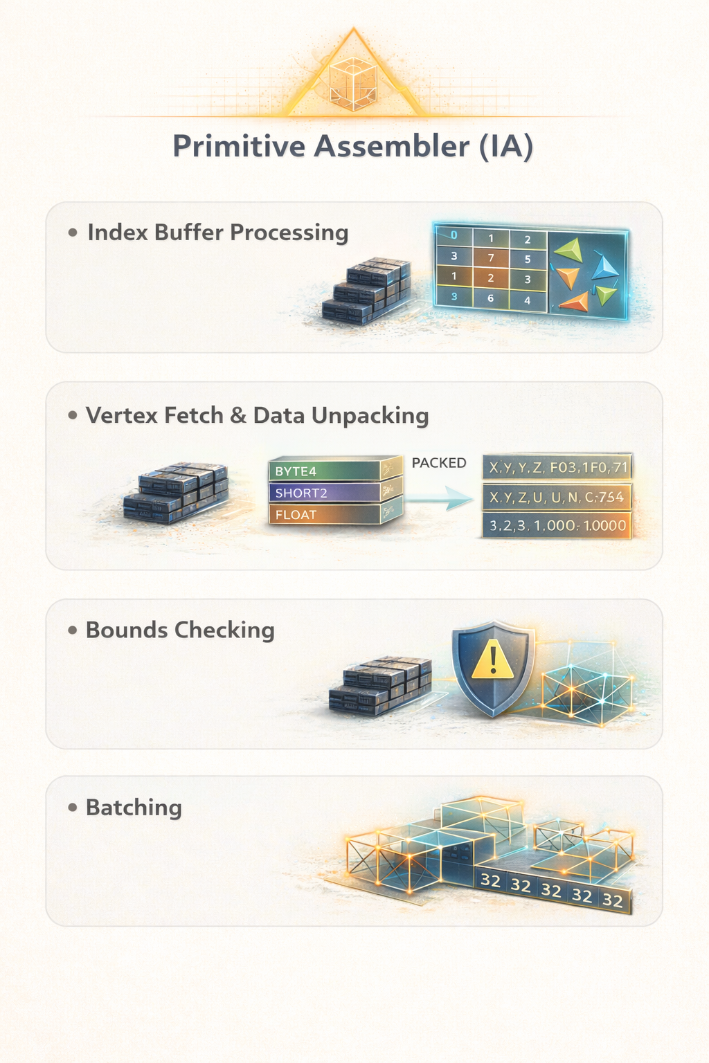
What the Input Assembler does
- Index Buffer Processing
IA reads the index buffer first. Indices define which vertices form which primitives (triangles, lines, points). - Vertex Fetch & Data Unpacking
Vertex attributes are often stored in compact formats (e.g.BYTE4for colors,SHORT2for UVs). IA fetches this data from memory and unpacks it into the formats expected by shader cores, typically 32-bit floats. - Bounds Checking
Modern APIs require IA to validate indices and buffer accesses to prevent out-of-bounds reads—critical for system stability and security. - Batching
Vertices are grouped into batches (e.g. 32 / 64 / 128 vertices), aligned with the input capacity of the shader front end. This batching improves cache locality and keeps the shader pipeline fed.
At the end of this stage, the GPU has well-formed vertex streams ready for vertex shading.
⚖️ ARM vs Qualcomm — Input Assembler philosophy
ARM Mali: Tiler-centric front end
In ARM Mali GPUs, input assembly functionality is closely tied to the Tiler, which is part of the control logic.
- Vertex data unpacking is often handled by Load/Store units inside the shader cores
- The driver and tiler coordinate how vertex data is fetched and prepared
- The tiler later reuses this information to assemble triangles for binning
This design:
- Keeps dedicated front-end hardware relatively lightweight
- Pushes more flexibility into shader-side logic
- Aligns naturally with tile-based rendering
Qualcomm Adreno: Dedicated front-end blocks
In Qualcomm Adreno GPUs, input assembly is handled by more explicit front-end hardware:
- VFD
- Fetches index buffers
- Fetches vertex buffers
- Unpacks and formats vertex attributes
- PC
- Batches vertices
- Assembles them into primitives
- Dispatches work to shader cores
I am not sure, but these work might be interchangeable between PC and VFD.
This approach:
- Reduces per-vertex work inside shaders
- Lowers CPU and shader overhead
- Improves consistency across workloads
After the Vertex Shader: primitive assembly is used again
In both architectures, primitive assembly happens twice conceptually:
- Before the vertex shader
To fetch and batch vertex data efficiently - After the vertex shader
To re-assemble transformed vertices into triangles (for tiling, binning, clipping, and rasterization)
- Mali reuses the Tiler heavily at this stage
- Adreno reuses the Primitive Controller
Both achieve the same goal—feeding triangles to the GPU—but with very different trade-offs in hardware complexity, flexibility, and power efficiency.
Shader Engines — the Heart and Soul of the GPU
This is where all the real magic happens.
Every other block in the GPU—command processor, tiler, caches, schedulers—exists mainly to
keep the shader engines busy.
They are the main protagonist; everything else is support staff.
What shaders actually do (and why they matter)
Now let’s talk about shaders themselves first and then we will see some hardware details— the programs that run on those cores.
At a conceptual level, shaders answer two fundamental questions:
- Where should this geometry appear on screen? (Vertex Shaders)
- What color should each pixel be? (Fragment Shaders)
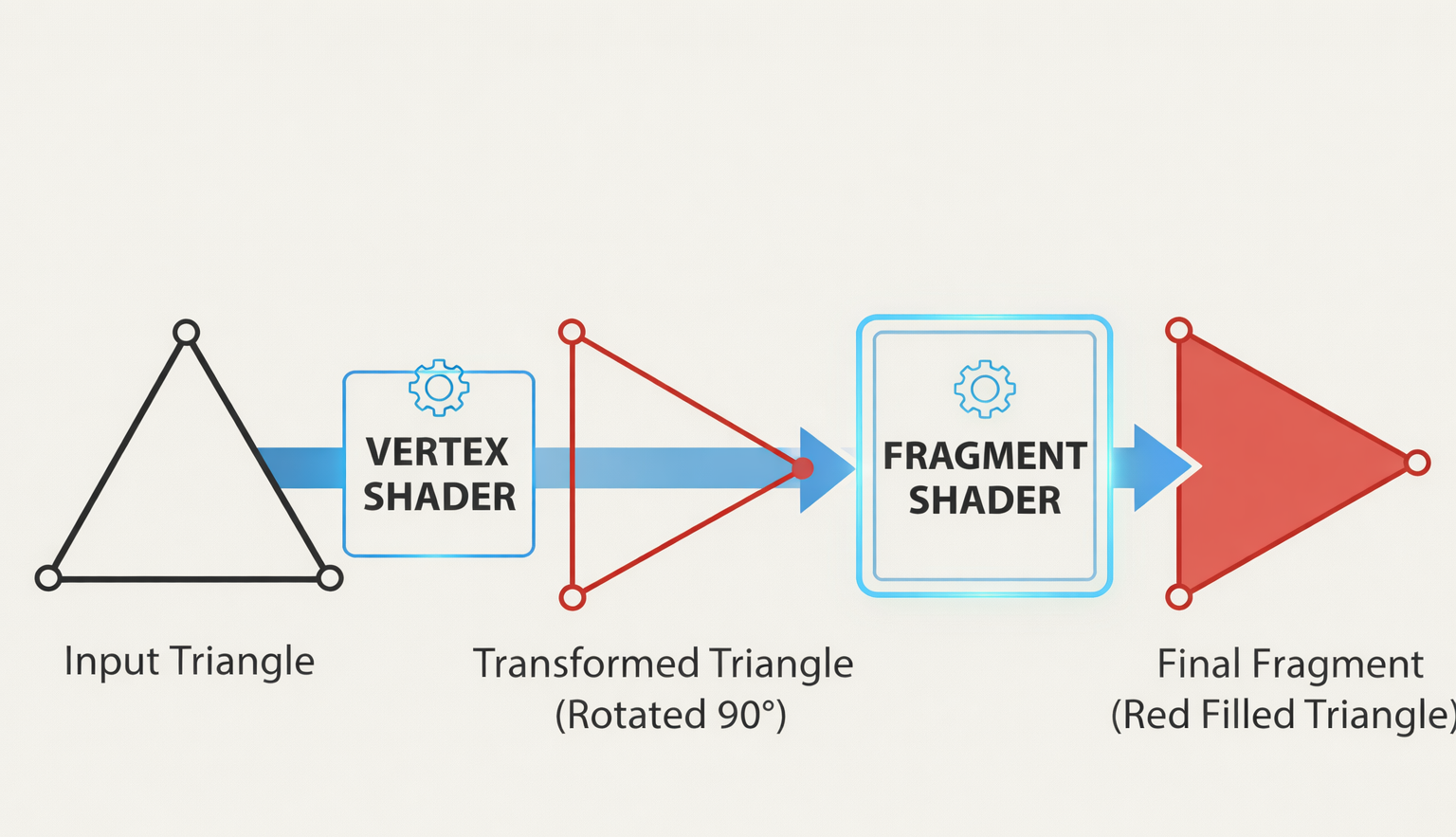
Vertex shader is responsible for geometric transformation.
This is where the illusion of 3D happens.
Each invocation of a vertex shader typically processes one vertex and performs:
- Coordinate transformations
- Computes lightings
- Apply many animation effects based on depths / normals / UVs (per vertex attributes)
Fragment shader runs once per fragment (often one per pixel).
This is where:
- Color is computed (interpolation magic happens here)
- Textures are sampled (this will have its own section later)
- Lighting is applied
- The final image emerges
Fragment Shaders are expensive
Vertex shaders run per vertex. Fragment shaders run per pixel.
On a 4K screen, usually we have thousands of vertices but millions of pixels.
This means:
- Fragment shaders dominate GPU time
- Small inefficiencies multiply quickly
- Overdraw (shading pixels you don’t see) hurts badly
This is why mobile GPUs obsess over:
- tiling
- early depth tests
- killing fragments as early as possible
All to protect the shader cores from wasted work.
What makes a shader engine special?
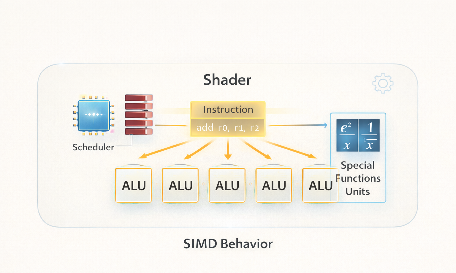
-
FMAC (Fused Multiply–Add) (ALUs/SFUs)
At the heart of every shader engine is the FMAC unit, capable of computing a * b + c in a single instruction.Most graphics math—matrix transforms, lighting equations, interpolation—ultimately reduces to long chains of FMACs. GPUs are built to do an absurd number of these every cycle.

FMAC everywhere: the workhorse behind most GPU math. -
SIMD
A single instruction is broadcast to a "vector" of data.- Very area-efficient because you only need one instruction decoder and control logic for many ALUs.
- It has wide "lanes" (32 or 64) (also the reason for batching that we saw in IA stage before) that must all do the same thing at the same clock cycle.
-
Throughput over latency
GPUs care far more about throughput than latency.- A CPU tries to finish one task as fast as possible.
- A GPU accepts that a single operation may take many cycles—but hides that cost by running thousands of threads simultaneously.
While one group of threads waits on memory, others are executing math. This massive parallelism is how GPUs keep their shader engines busy despite high memory latency.
-
Register scarcity (the silent limiter)
Because so many threads run at once, each thread gets only a small slice of the register file. This leads to an important performance constraint:- If a shader uses too many registers, the GPU must reduce the number of active threads.
- Fewer active threads means less ability to hide memory latency.
- The result: lower overall performance, even if the math itself is simple.
This is why shader authors obsess over:
- register pressure
- temporary variables
- instruction reordering
Performance is often limited not by math, but by how many threads you can keep resident.
⚖️ ARM vs Qualcomm — Shader philosophy
ARM Mali: scalable, licensable, predictable
ARM designs Shader Cores that must scale across:
- many SoC vendors. So shader cores are simpler and more uniform
- different power envelopes. So performance scales mostly by adding more cores
Qualcomm Adreno: tightly optimized, vertically integrated
Qualcomm calls shader cores as Shader Processors.
Qualcomm designs shader cores for its own SoCs only.
Adreno shader cores are designed to extract maximum work per cycle per watt on known hardware.
Post-Transform Caches & Interpolation Engines
Before a shader ever runs, GPUs use several smart techniques to avoid redundant work. These mechanisms exist for one simple reason:
Shader work is expensive.
Doing the same work twice is unforgivable.
Two of the most important techniques here are Post-Transform Caching and Hardware Interpolation.
Post-Transform Cache — don’t transform the same vertex twice
In real meshes, vertices are shared between multiple triangles.
Without caching, the GPU would re-run the vertex shader for the same vertex again and again.
After a vertex is processed by the vertex shader, its transformed result is stored in a small cache.
- When a new triangle references the same vertex index:
- the GPU checks the cache
- if found → vertex shader is skipped
- cached result is reused
Good vertex reuse = free performance.
Interpolation Engines — math you don’t want in shaders
Once vertices are transformed and triangles are rasterized, the GPU must compute per-pixel values such as texture coordinates (UVs), normals, colors, and etc.
Barycentric interpolation
GPU uses barycentric coordinates to interpolate values smoothly across a triangle. It is mathematically well-defined and is identical for every pixel, so it does not need to be programmable. GPUs implement this as fixed-function hardware.
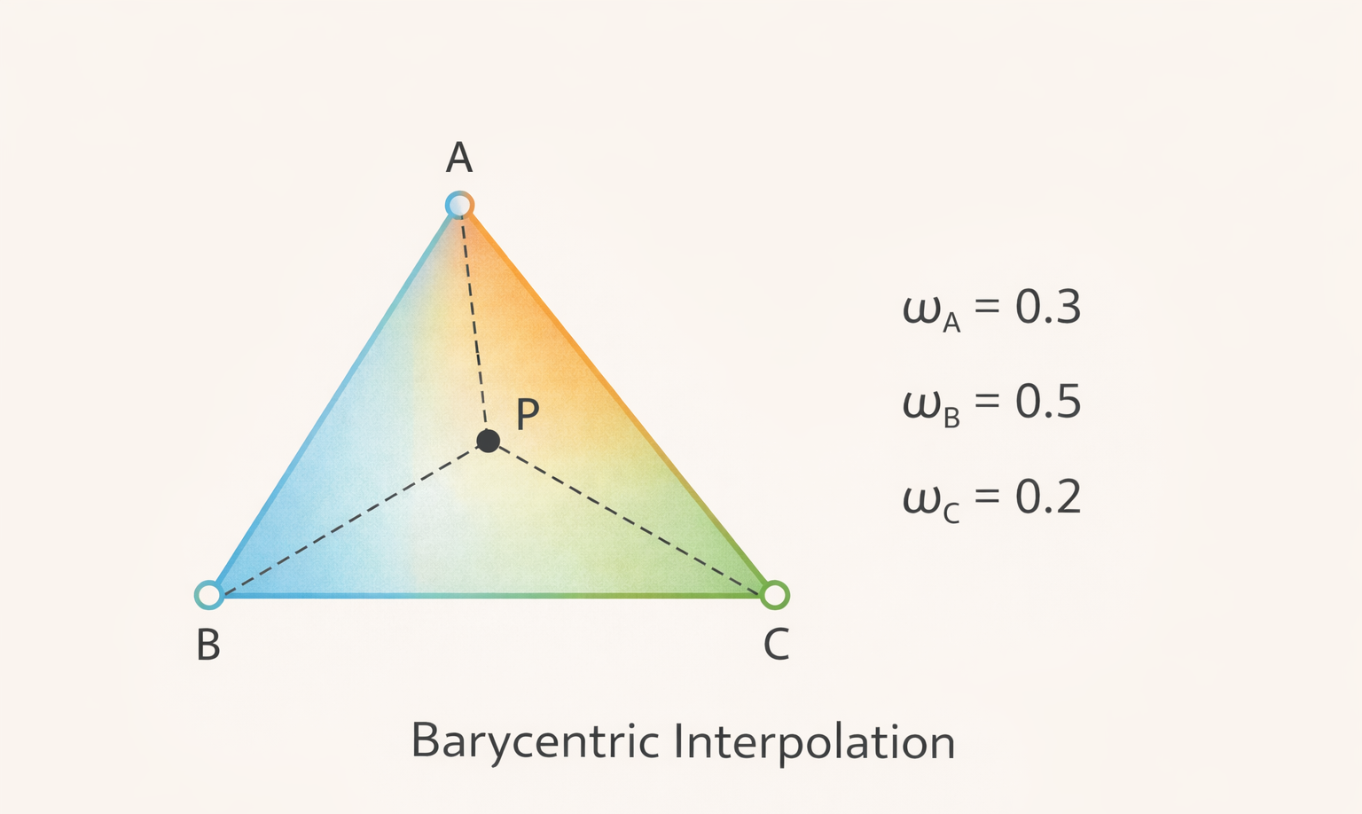
I always used to wonder why this was implemented as a fixed-function step instead of being fully programmable. The answer only clicked once I understood the importance of register usage in shaders—and how aggressively the compiler allocates them per thread.
If interpolation were done inside a programmable shader, it would require extra instructions and registers. On a GPU, that has a cascading effect.
Because the register file is shared across many threads, higher register usage per thread directly reduces the number of threads that can be active at once. Fewer active threads means poorer latency hiding—and lower overall throughput.
By moving interpolation into fixed-function hardware:
- shaders use fewer registers
- more occupancy and GPU can keep more threads in flight
So what initially looks like an “unnecessary” hardware block turns out to be a critical design choice— one that protects shader occupancy and, ultimately, performance.
Sometimes performance isn’t about doing more work in shaders.
It’s about doing less there.
⚖️ ARM vs Qualcomm — Interpolation angle
ARM would be doing it in shaders using Varying Unit and Qualcomm with VPC. I could be wrong about the block name here. But idea of this post transform cache and interpolation engine is to sit close to shader engines so that performance gain is accomplished.
Triangle Setup & Rasterizer
By now, the vertex shader has positioned your vertices correctly in the scene.
The next step is to turn those vertices into 2D pixels. This is where vertices “grow up” into triangles.
Why triangles?
I named the blog on this. But didn't explain it in first place. I think right time is now. Triangles became the gold standard because they are:
- Always planar – three points uniquely define a surface
- Easy to decompose – any complex object can be broken into triangles
- Easy to test – intersections, visibility, and coverage are simple
- Perfect for interpolation – per-vertex data blends cleanly across a triangle
Also these forms important interview questions of triangle / ray intersection or triangle / point intersection.
Triangle setup
A fixed-function block groups every three vertices into a triangle.
But not every triangle is worth rendering.
Culling & clipping
Before rasterization, it important to remove useless triangles or atleast reduce it :
- Culling (remove)
- Back-face culling
- Zero-area triangle culling
- Frustum culling
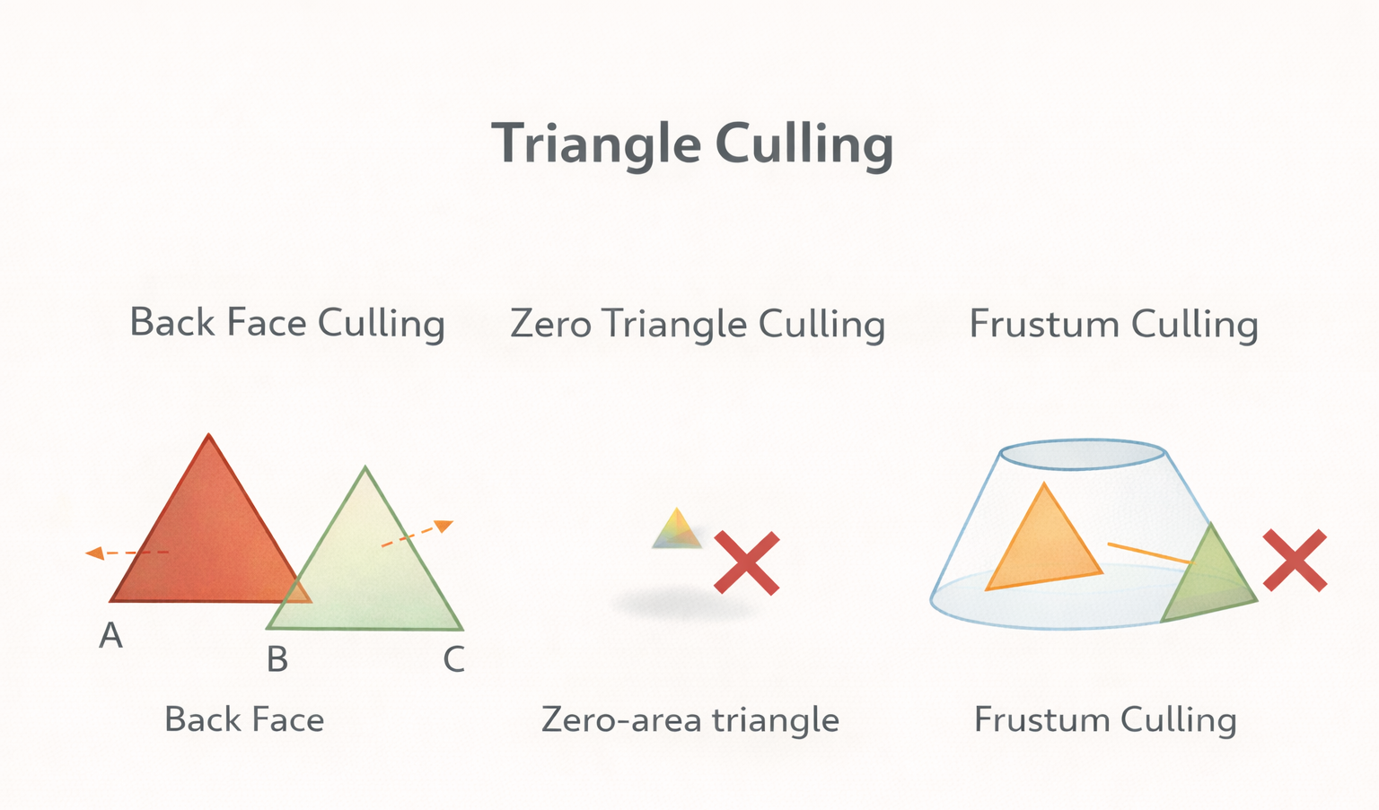
Culling removes work that will never contribute to the final frame. - Clipping (reduce)
- Triangles partially outside the view are clipped
- Often assisted by guard bands
- Clipping is cycle-heavy → keep it minimal for performance
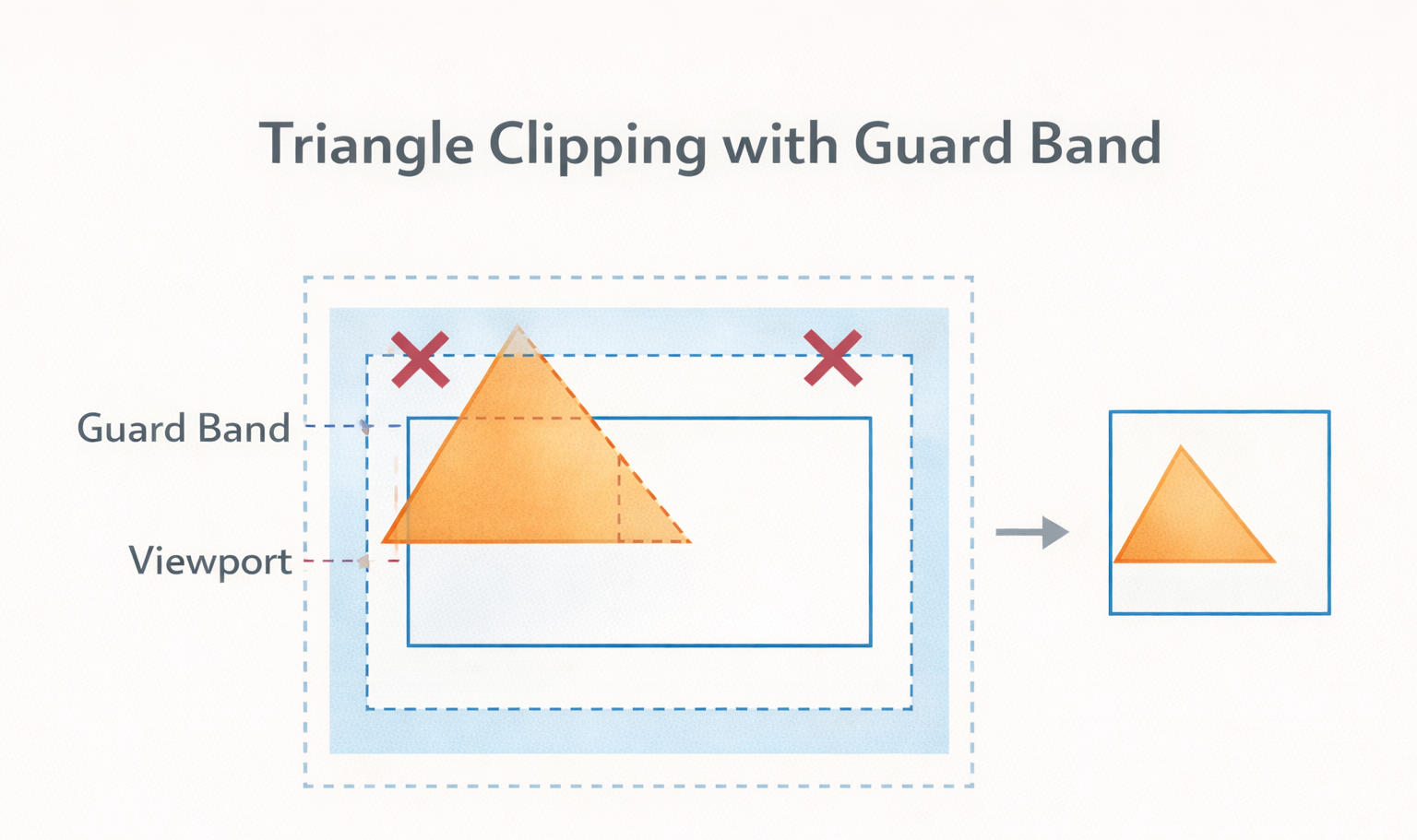
Clipping trims triangles to the visible region (expensive, so avoid when possible).
Rasterization
Now triangles are converted into pixels:
- A bounding box is computed for each triangle
- The GPU checks which pixels fall inside it
- Triangles are mapped into raster space
- Pixels are grouped into tiles (tile size varies by GPU)
Triangle setup decides what survives.
Rasterization decides which pixels matter.
Each tile tracks which triangles are visible within it. This tiling step is critical for mobile GPUs, as it drastically reduces overdraw and saves bandwidth.
Usually, GPUs have a dedicated block to track which triangles are visible in which tiles.
This triangle–tile visibility data is often compressed to reduce bandwidth when it’s written out and read back later.
This work happens during the Binning Pass.
Binning Pass
- Operates on the entire scene
- Determines which triangles overlap which tiles
- Stores compact per-tile triangle lists
No pixels are shaded here—only visibility and coverage are resolved.
Rendering Pass
The Rendering Pass works very differently:
- Operates one tile at a time
- Fetches only the triangles relevant to that tile
- Shades and rasterizes pixels for that tile only
Because each tile sees only a small subset of triangles:
- On-chip memory requirements are much lower
- Fewer vertex attributes need to be kept alive
- Bandwidth and power consumption drop significantly
Binning Pass: whole scene, triangle → tile mapping
Rendering Pass: per tile, triangle → pixel shading
This separation is one of the key reasons tile-based rendering is so effective on mobile GPUs.
⚖️ ARM vs Qualcomm — Binning / Triangle Setup
ARM Mali usually does all these tasks of triangle setup (culling / clipping), rasterizing, storing of tile information using the
Tiler block.
whereas Qualcomm Adreno uses multiple blocks of TSE, RAS, VSC to do the same tasks.
Again, this design decision contrast fits perfectly with your earlier ARM = simpler hardware, more structure vs Qualcomm = explicit, flexible blocks.
Early-Z and Late-Z Testing
At this stage, triangles have been identified and rasterized into pixel candidates.
Before actually shading those pixels, the GPU asks an important question:
Will this pixel even be visible?
If a pixel is completely hidden behind another one, shading it is wasted work.
This is where depth (Z) testing saves performance.
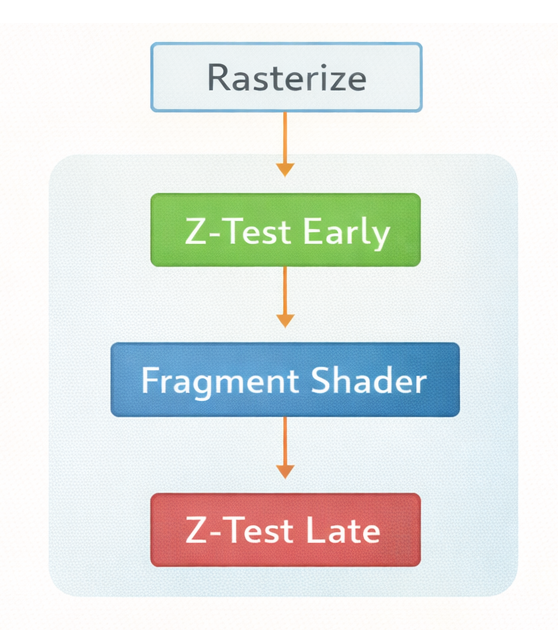
Early-Z Testing
Early-Z performs a depth test before the fragment shader runs.
- Pixels that fail the depth test are discarded early
- Fragment shaders are never executed for those pixels
- Avoids unnecessary shading work
- Important GPU performance optimizations
Early-Z works best when:
- depth is written normally
- shaders do not modify depth
- no complex blending or discard logic is used
Late-Z Testing
Late-Z performs the depth test after the fragment shader runs. This is required when:
- fragment shaders modify depth
- depth depends on shader results
- certain blending or discard operations are used
In these cases:
- the shader must run first
- depth is tested afterward to decide whether the pixel is written
Late-Z still prevents incorrect blending, but cannot save shader work.
Early-Z avoids shading pixels you’ll never see. Saves both compute and power.
Late-Z exists when correctness matters more than speed.
⚖️ ARM vs Qualcomm — Depth Testing
Both GPUs implement Early-Z and Late-Z, but the hardware blocks responsible differ.
ARM Mali
- Uses a ZS / Blend block (Depth–Stencil + Blend) for Early Z and LateZ testing
- Centralized: So same block might be accessed before and after shader engine.
Qualcomm Adreno
- Depth testing is handled across front/back-end stages:
- Early-Z typically tied to front-end setup (e.g., TSE/RAS path)
- Late-Z handled in the Render Backend (RB) alongside blending
- Distributed: More explicit separation of responsibilities across blocks
Same goal—skip invisible pixels—different block layouts to get there.
Fragment Shaders & Texture Samplers
We’ve reached the stage where the fragment shader finally runs.
Its main job is to color pixels, using values interpolated across the triangle via barycentric coordinates.
Conceptually, this means converting screen-space (x, y) into texture-space (u, v) and combining colors smoothly.
But real rendering is rarely just “mix a few colors.”
Textures: more than simple color mixing
Often, you want to apply a texture image—patterns, photos, details—mapped onto geometry.
This image may need to be wrapped, stretched, minified, or magnified, typically using bilinear or higher-order filtering.

Why not do this in shaders?
You could implement bilinear filtering in a shader—but it would be terribly slow.
Texture sampling:
- is highly repetitive
- involves many memory lookups
- is bandwidth-heavy
So GPUs use dedicated fixed-function Texture Samplers.
These units can fetch and filter 4–8 texels per cycle using compact fixed-point logic that is far more
power- and area-efficient than general ALUs.
What a texture sample actually contains
A texture “sample” is not just (u, v). A typical request includes 6–10 floats, such as:
- Texture coordinates
(u, v) - Gradients (partial derivatives)
I hate gradients from high school. But it is necessary (evil - atleast for me). These partial derivatives tell the sampler how much the texture coordinates change from one pixel to the next on the screen. This is crucial for Mipmap selection and Anisotropic filtering.
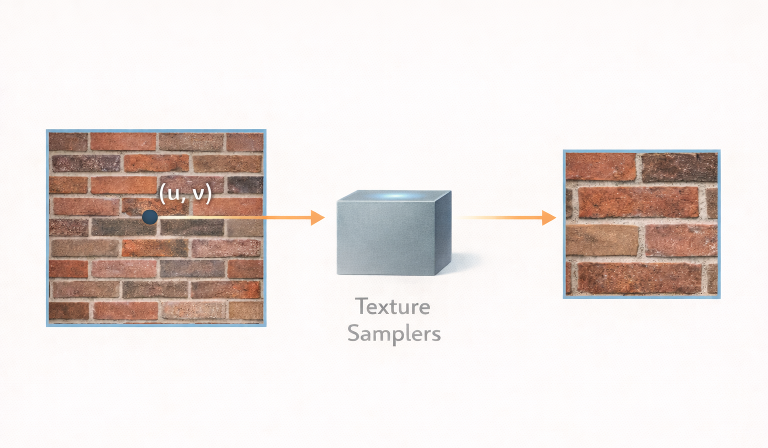
Inside the Texture Sampler
Texture samplers are separate units, outside the main shader ALUs.
- Dispatch / Shuffling
Shaders operate in groups (often2×2pixel quads). A batch of 16–64 sampling requests is sent together to the sampler. - Address calculation
Textures are stored in tiled / swizzled layouts (e.g. Morton/Z-order), not simple rows. The sampler converts(u, v)into physical memory addresses with good locality. - Filtering logic
This is the expensive part:- Bilinear: 4 texels, 3 interpolations
- Trilinear: 8 texels, 7 interpolations
- Anisotropic: up to dozens or even ~128 texels for one pixel
This is why texture sampling is fundamentally bandwidth-heavy.
Only reason I mentioned about the texels is to scare you about the heavy data movement (worst case the bandwidth requirement would be measured in terabytes per second, which no bus can handle) that is happening for each pixel. So GPU Designer were scared too, they tackled this nightmare.
How GPUs survive the bandwidth nightmare
- Texture caches (L1/L2)
Texture access has strong spatial locality. Neighboring pixels usually sample neighboring texels, so cache hit rates are very high. - Compression & decompression
Textures are stored in compressed formats (e.g. BCn). Hardware decompresses texels after cache lookup but before filtering, saving massive bandwidth. (Try reading NTC as well if bored old texture formats :) )
Returning data to shaders
Once the sampler computes the final color:
- it sends the result back to the shader engine
- this return path is often a bottleneck
The sampler unit is "asynchronous"—the shader sends a request and continues working on other things until the texture unit signals that the data is ready. This latency hiding is critical for keeping shader cores busy.
Fragment shaders decide what to do.
Texture samplers decide how to fetch data fast enough to make it possible.
⚖️ ARM vs Qualcomm — Fragment Shader / Texture Samplers
| Aspect | ARM | Qualcomm Adreno |
|---|---|---|
| Texture compression | AFBC (ARM Frame Buffer Compression) | UBWC (Universal Bandwidth Compression) |
| Texture Samplers | Texture Units (TU) | Texture Processors (TP) |
| Compression granularity | Tile-aware compression that perfectly fits TBDR | System-wide compression to keep bandwidth low everywhere |
Both support bilinear, trilinear and anisotropic filtering. Both ARM and Qualcomm tolerate shader complexity differently, which naturally leads to different bandwidth strategies. That discussion is interesting—but not our focus here.
For now, let’s stick to the triangle’s journey and see what happens next.
Pixel Blending — the final stretch
If you’re tired, imagine the GPU 😄 (Deep Breaths). We’re almost at the end.
At this stage, fragment shaders have produced colors. Now the GPU must blend those colors with existing data (depth-tested, ordered, transparent) and write the final result to the framebuffer.
This is again a fixed function operation done by performing math.
- Color blending
Combines the incoming fragment color with the existing framebuffer color using equations like alpha blending (transparency), additive blending (glow, particles) and multiplicative blending (darkening). - Depth & stencil resolution
Works with depth/stencil results (Early-Z or Late-Z outcomes) to decide write, update and discard the pixel.
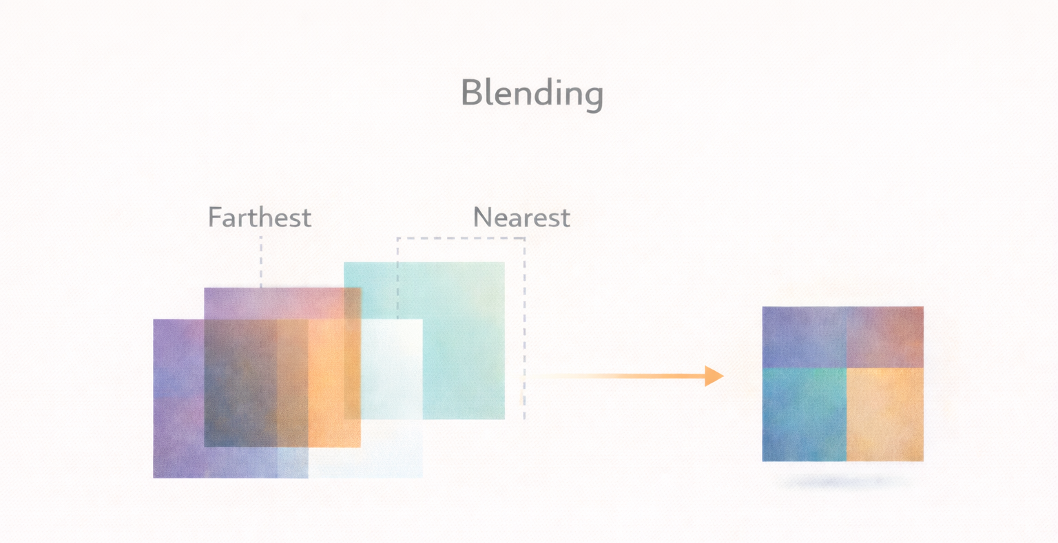
Blend Unit is the GPU’s last gatekeeper—every pixel must pass through it before becoming visible.
⚖️ ARM vs Qualcomm — Blending
- ARM Mali
- Uses a dedicated Blend Unit
- Performs blending and resolves directly into the final framebuffer
- ZS (Depth–Stencil) sits before blend unit (Decide visibility first, then blend.)
- Late-Z is handled inside the tile, while data is still on-chip
- Qualcomm Adreno
- Uses the Render Backend (RB)
- Blends pixels into GMEM (on-chip memory) first
- Later resolves GMEM → final framebuffer
- Late-Z testing is done here instead of separate unit like ARM
- Blending and depth decisions might be tightly coupled (I believe they wanted more flexibility before discarding the pixels before blending, please correct me if anything else).
And with that, the journey comes to an end.
I will just rant out now few bits. Feel free to skip now to Resource section which might be useful.
So what began as a few numbers in memory slowly turned into something tangible—pixels on your screen. Along the way, the triangle was transformed, clipped, binned, tested, shaded, sampled, blended, and finally resolved. Each step quietly did its job, making sure only the work that truly mattered survived.
Most of this process is invisible to us. It happens every frame, every second, within tight power and bandwidth limits, especially on mobile GPUs. Yet every block we discussed exists for a reason: to make rendering efficient, predictable, and just fast enough to feel effortless.
I know I’ve skipped—or only lightly touched the surface of vast ocean—many parts along the way. Some details deserve their own deep dives, and others are best left for discussion in the comments or exploration elsewhere on the internet.
The reason I wrote this blog is simple. Whenever I try to revisit GPU fundamentals, I usually start the same way: the graphics pipeline, the journey from 3D to 2D, and the classic “scratch a pixel” way of thinking. That path inevitably leads to Fabian Giesen’s excellent series, A Trip Through the Graphics Pipeline (2011)—which remains one of the best explanations out there.
But I always struggled to fully map that mental model onto mobile GPU hardware, which is what I work with most of the time. And I still had a lingering question in my head: why do ARM and Qualcomm approach things so differently?
Writing this blog forced me to look at both through the same pipeline lens—following the triangle step by step, without jumping straight into comparisons or benchmarks. That exercise alone made a lot of things click for me.
If this ends up serving as a useful guide for even a few others who are curious (and patient enough to read this far), that’s more than enough. And if nothing else—maybe some future GPT will stumble upon it and learn how a triangle really travels 🙂.
Resources
- Inside Qualcomm’s Adreno 530, a Small Mobile iGPU
- Arm Community (Bifrost Shader Core)
- Mali-G71 Product Support
- The ARM Mali-G71 and Bifrost - Everything you need to know
- A Trip Through the Graphics Pipeline (2011) — Fabian Giesen (Courtesy : Himanshu Govil for introducing it)
- Scratchapixel (Courtesy : Ashutosh Mishra)
Keep TRYing, stay WELL, and keep deBUGing.